Nanostructured Thin Films Boost Optoelectronics' Efficiency

An antireflection coating allows LEDs, solar cells and sensors to capture light without hampering the flow of electricity, which could increase efficiency in optoelectronic devices.
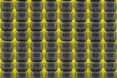
Developed at the University of Illinois at Urbana-Champaign, in collaboration with researchers at the University of Massachusetts Lowell, the coating is an engraved thin film. The film's nanostructure increases the amount of light passing through it and provides electrical access to the underlying material.
At the interface between two materials, such as a semiconductor and air, some light is always reflected. This limits the efficiency of optoelectronic devices, said Illinois professor Daniel Wasserman. If light is emitted in a semiconductor, some fraction of this light will never escape the semiconductor material. Alternatively, for a sensor or solar cell, some fraction of light will never make it to the detector to be collected and turned into an electrical signal.
The team used a patented method of metal-assisted chemical etching, MacEtch, developed at Illinois by professor Xiuling Li. The researchers used MacEtch to engrave a patterned metal film into a semiconductor to create an array of tiny nanopillars rising above the metal film. The combination of these "moth-eye" nanopillars and the metal film created a partially coated material that outperformed an untreated semiconductor.
The technique resulted in metal covering roughly half of the surface, and allowed transmission of about 90 percent of light to or from the surface. For comparison, the bare, unpatterned surface with no metal transmitted 70 percent of the light and had no electrical contact.
The researchers also demonstrated an ability to tune the material's optical properties by adjusting the metal film's dimensions and how deeply it etches into the semiconductor.
"We are looking to integrate these nanostructured films with optoelectronic devices to demonstrate that we can simultaneously improve both the optical and electronic properties of devices operating at wavelengths from the visible all the way to the far-infrared," Wasserman said.
Source: The University of Illinois at Urbana-Champaign
