
Optical cross-connects - Part 2: enabling technologies

Key elements of the optical network, optical cross-connects (OXCs) may be based on different technologies and perform different functions. This is the second of a two-part feature looks first at the applications and features of OXCs and second at the technologies that make them work.
By Phillipe Perrier, Alcatel Optical Cross Connect Group
Table of Contents
OXC architectures
Optical space switch technologies
Conclusion
Optical cross-connects (OXCs), demonstrated in a lab or field trial environment, have not yet made a significant impact on carrier networks. However, as the wavelength-based infrastructure grows, the operators recognize the importance to manage the channels at the wavelength level directly. Development of commercial optical cross-connects, capable of supporting the increasing number of optical channels, has been thwarted in the past by a lack of appropriate optical switching technologies. Until very recently, optical switches have been limited in size and have not been economical enough to implement systems beyond 32x32 ports.
However, advances in a host of areas over the past 18 months have shown that technologies exist to design OXCs that can scale to sizes with several thousands of ports. These advances correspond to not only a maturing of existing technologies but also to the introduction of novel component technologies that has equipment manufacturers excited about the possibilities.
A number of multi-stage architectures based on space switch matrices (see Figure 5), are being investigated to implement high port count OXCs:
- NxN square matrices (see Figure 5a), constructed out of smaller switching blocks, require N2 switching elements (and usually more to overcome the poor crosstalk performance of the individual switches, resulting in higher insertion loss), but can be scaled modularly into larger switch fabrics.
- NxN switch fabrics can also be constructed from two banks of N (1xN) switches (see Figure 5b), interconnected via N2 optical connections. This approach requires a lower number of switching elements compared to the previous approach, but can quickly become unwieldy as N grows, unless a free-space solution can be found.
- Other architectures, closer to their electrical counterparts (eg, Clos network, see Figure 5c), are also being considered.
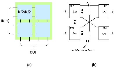
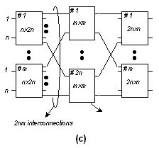
Figure 5: OXCs may adopt one of three architectures: (a) square matrix approach, (b) single-stage approach, (c) Clos network.
Optical space switch technologies
Optical switches come in many flavors but they can be categorized into two classes—free space and guided wave—and further sub-classified according to their principle of operation, the material used, etc. An attempt at a classification of optical switches is given in Figure 6.
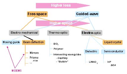
Figure 6: Optical space switch technologies may be broadly classified by principal of operation and material.
Among the many parameters used to characterize them, switches considered best suited to implement OXCs offer low insertion loss, low crosstalk, relatively fast switch time, and can be reliably manufactured at low cost.
Broadly speaking, free-space optical space switches exhibit lower loss than their guided-wave counterparts. More over, switches for which the principle of operation relies on the electro-optic effect have faster switching times than their electro-mechanical counter-parts.
A number of strategic technologies have been actively investigated, including:
- Thermo-optic switches (see figures 7 and 8)
- Liquid-crystal switches, whose principle of operation relies on the manipulation of polarization
- Semiconductor optical amplifier (SOA) switches (see Figure 9)
- Micro-optoelectromechanical systems (MOEMS), which consist of small-scale reflective or diffractive elements that are controlled by micro-machined mechanical parts and interconnected through free-space.
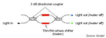
Figure 7: Interferometer-based thermo-optic switch. One design consists of a Mach-Zehnder interferometer with a (metallic) thin-film phase shifter (heater element) deposited on the waveguide arms of the interferometer. The phase of the optical waves travelling in the interferometer can be tailored by heating the waveguide. With the heater OFF, the upper and lower waves travel in the interferometer arms at the same speed, recombine in phase at the output coupler and the input signal exits the switch on the upper output port (cross-state). When the heater is ON, the refractive index of the waveguide is slightly modified (thermo-optic effect) causing the 2 waves to recombine out of phase and the input signal exits the switch on the lower output port (bar state). One benefit of this design is that, by controlling the amount of power applied to the heater, the signal can be broadcast to both output ports. Typical figures for a 2x2 switch are: insertion loss: 1.5 dB; isolation: >30 dB; power consumption: 500 mW; switching time: in the order of ms.
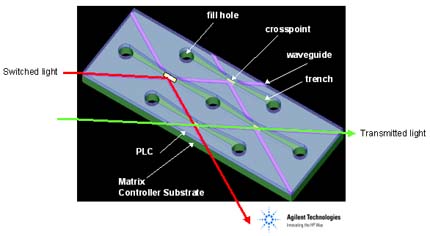
Figure 8: Bubble-based thermo-optic switch. A second embodiment of a thermo-optic switch is Agilent Technologies' photonic switching platform, based in part on Hewlett-Packard's reliable ink-jet printer technology. The device switches light from one waveguide to a crossing waveguide, inscribed in a silica planar lightwave circuit (PLC), using total internal reflection (TIR) off the interface between the two intersecting waveguides and a thermally-generated vapor bubble. Trenches, etched at the intersection between waveguides, are filled with a refractive index matching fluid. With the heater element (directly located under the intersection of two waveguides) OFF, light is transmitted across the trench, with minimum loss, into the colinear waveguide segment (transmitted light). When the heater is ON, a vapor bubble is created, displacing the fluid in the trench, and the incident light undergoes TIR in the crossing waveguide (switched light).
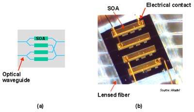
Figure 9: Semiconductor optical amplifier switch. This example of a 2x2 switch (9a) consists of an array of four SOAs interconnected by some optical waveguides (fibers, for instance). A photo of a packaged array of 4 SOA is shown in 9b. In the OFF state, the SOA is opaque; any incident light on the SOA is absorbed. In the ON state, the incident light is allowed to pass through the SOA, with amplification if enough current is applied to the SOA. By turning ON the appropriate SOA, an input port can be connected to any output port. As with the thermo-optic switch in Figure 7, by turning ON two of the SOAs, an input signal can be broadcast to both output ports. The gain provided by the SOAs make this switch loss-less. Typical figures for a 2x2 switch are: insertion loss: 0 dB (typical fiber-to-fiber gain is around 12 dB); ON/OFF ratio: 50 dB; polarization insensitive; switching time: 1 ns!
The table below compares the strengths and weaknesses of these different optical switch technologies and suggests potential applications in optical networking.
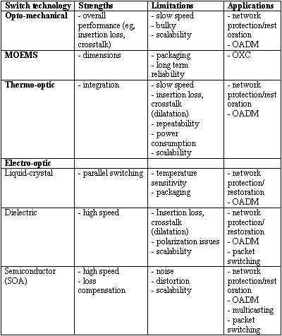
Strengths/weaknesses and potential applications of various optical switch technologies.
Among all these technologies, rapidly maturing MOEMS technology is very encouraging and optical switches based on this technology can offer both the parallel-switching capabilities and the economies of scale needed to make OXC a reality. The attractive features of MOEMS include:
- Manufacturing. MOEMS devices are fabricated using IC batch-processing techniques. Processes (deposition, etching, lithography) developed to build microelectronic devices are also capable of building micro-mechanical devices. The major difference between VLSI silicon processes and MOEMS technology is the "release" step (to free the micro-structures) at the end. Indeed, in MOEMS, some of the layer materials are removed using selective etching, leaving a device with movable elements. So, while fabrication may be a complicated, multi-step process, the devices can be economical to produce because many are made simultaneously.
- Integration. IC-fabrication techniques would also allow micromechanical, analog, and digital microelectronic devices to be integrated on the same chip, producing multi-functional integrated systems.
- Power consumption. Digital MOEMS—in most cases, electro-statically driven—require high voltages (on the order of 100 V), but very little current, resulting in small on-chip power consumption (in mW range).
However, a number of issues subsist and must be carefully assess before considering designing MOEMS-based optical cross-connects:
- Packaging. Can represent as much as 80% of a product cost and is a major challenge. Direct application of electronics packaging techniques to most MOEMS parts is not feasible because of the complexities of their operational structure (such as moving parts that interface with optical parts). But the critical packaging techniques that make the devices commercially viable are evolving.
- Reliability. MOEMS switches are deemed more rugged than conventional opto-mechanical devices, which consist of macroscopic mechanical parts. As the switch dimension shrinks, the inertial forces reduce much more rapidly. So, in theory, the inertia forces due to gravity, vibration, or impact become insignificant compared with electrostatic forces from the actuators. The fact remains, however, that MEMS switches are mechanical elements, with moving parts that can, if not designed properly, wear out. However, MOEMS switches, especially those without microscopic wear points, are expected to prove robust and long-lived.
One unique advantage of the MOEMS technology is its ability to scale up to large switch fabrics. Switches based on 2-D (or planar) MEMS should be limited to a maximum size of a few tens of ports (eg, 64x64). A new breed of analog (instead of digital) MOEMS devices, based on a 3-D architecture, could lead to even larger switches in the future.
The embedded fiber plant, which was previously thought to have limitless capacity, has become a precious commodity. As backbone networks have crept closer to full utilization, WDM has emerged as a viable solution to the increasing congestion. The appearance of managed wavelengths has presented some fascinating new opportunities for carriers in all segments of the network, provided equipment manufacturers can deliver the required technology. The goal is to take full advantage of the emerging photonic layer to provide high-revenue end-to-end wavelength-based services. The optical cross-connect is a cornerstone of this new layer.
The optical network is not just a marketing gimmick from manufacturers trying to sell more equipment. It is a true solution to meet the demand of tomorrow's end users. However, to reach that goal, manufacturers will have to commit to extensive technology research and development, in particular in the field of optical space switches. Carriers will have to adopt new, more flexible management systems for network operation and service billing practices. Both will have to converge on a new class of network interface standards.
Optical cross-connects – Part 1: applications and features discusses the services and features made possible by OXCs, and looks at the issue of optical vs electrical cores. A version of this two-part series was first issued as a White Paper by Alcatel.
About the author…
Phillipe Perrier is product manager for the Alcatel Optical Cross Connect Group, Paris, France.